Search...
What Are You Looking For?
Tungsten is an important refractory metal with the characteristics of high melting point, high density, high strength, good thermal conductivity and low thermal expansion coefficient. It is widely used in aerospace, military weapons, electronics and nuclear industries [1,2]. In the International Thermonuclear Reactor, tungsten is identified as the best choice for plasma materials due to its outstanding advantages such as good heat resistance, high sputtering threshold and low activity under neutron irradiation [3]. However, due to its high melting point (3410 ℃) and room temperature brittleness [4], tungsten is difficult to prepare and process by traditional casting or machining methods. Usually, tungsten metal parts are prepared by powder metallurgy, but sintered tungsten materials have the disadvantages of poor performance, low relative density and difficult to control impurity content, which makes it difficult to meet the needs of modern high-tech development.
In recent years, with the continuous expansion of the application field of pure tungsten materials, the design requirements for parts are getting higher and higher. In armor-piercing shells, rocket nozzles, and nuclear fusion devices, the required tungsten parts usually have complex structures such as inner holes, curved surfaces, and grooves. This requires tungsten metal parts to develop towards a higher degree of manufacturing freedom in three-dimensional shape design. However, traditional forming methods have limitations in manufacturing parts with complex structures [5]. Since additive manufacturing technology can produce components with complex geometric shapes, it is a good choice for tungsten material processing. This technology has received widespread attention in opening up new applications for tungsten [6,7]. However, the inherent brittleness of tungsten and the microcracks generated during the additive manufacturing process will damage its structural integrity, hindering the development and application of tungsten metal additive manufacturing. At present, the research mainly focuses on exploring the manufacturing of pure tungsten and tungsten alloys through powder bed selective laser melting technology (SLM) and selective electron beam melting technology (SEBM) [8,9]. On the one hand, SLM technology is used to characterize the formation mode and principle of microcracks during tungsten additive manufacturing, and to develop specific printing process parameters suitable for tungsten alloy materials [10,11]. On the other hand, the energy advantage of SEBM additive manufacturing technology, namely electron beam, and the ability to preheat metal powder and carrier plate before melting, thereby reducing deformation and internal stress, can be used to manufacture tungsten materials that are brittle at room temperature [12,13].
In this study, pure tungsten was prepared by SLM and SEBM technology, and the effects of printing process parameters on the macro/microstructure and mechanical properties of pure tungsten were compared. The crack initiation location and formation mechanism were analyzed by focusing on characterization techniques such as SEM and EBSD. The comparison of the organizational characteristics of the two preparation processes has important guiding significance for obtaining tungsten materials with high density and few cracks. At the same time, the research on the process parameters and crack formation mechanism of pure tungsten additive manufacturing also has extensive processing and application significance for the preparation of other materials with high melting points, such as niobium and molybdenum.
1 Experiment
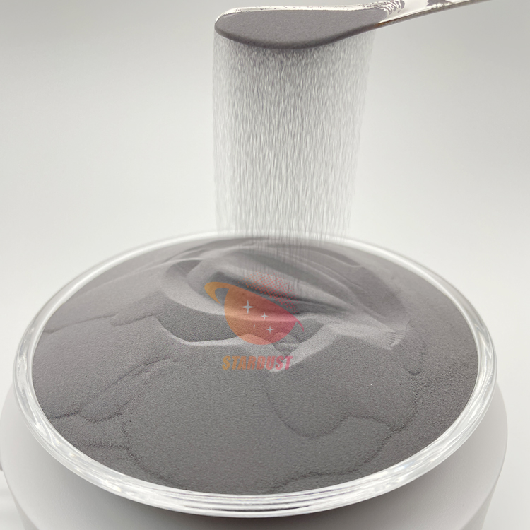
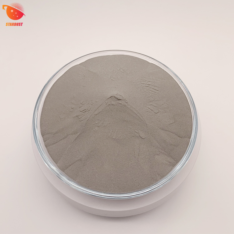
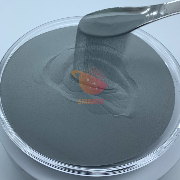
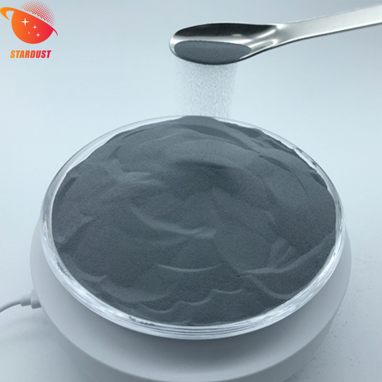
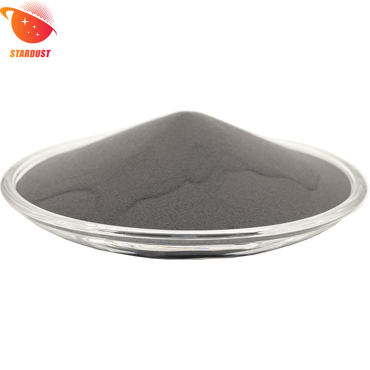
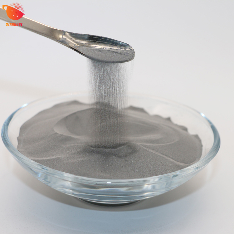
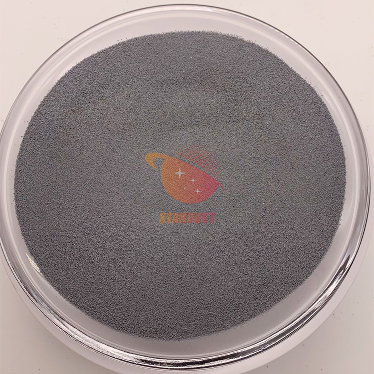
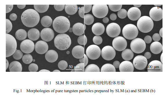
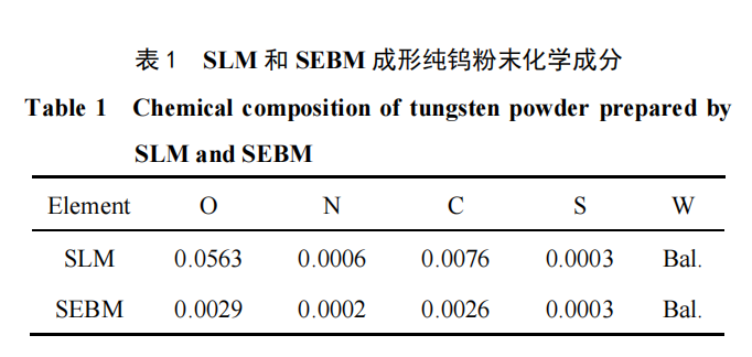
The tungsten powders formed by SLM and SEBM are both spherical powders, but due to the differences in the melting capacity and forming process characteristics of the two equipment, their particle size distributions are different. The powder used for SLM forming was purchased from the reduced tungsten powder generated by Sichuan Zigong Cemented Carbide Company. After plasma spheroidization treatment, it became spherical tungsten powder. The powder morphology is shown in Figure 1a. The powder particle sizes D10, D50 and D90 are 5.3, 11.5 and 25.0 μm, respectively. SEBM printing equipment needs to use coarser powder to prevent the "flying powder" phenomenon during the forming process. The morphology of the powder is shown in Figure 1b. Its D10, D50 and D90 are 52.4, 81.1 and 123.0 μm, respectively. The chemical composition of the two tungsten powders is shown in Table 1, and the purity is greater than 99.9%.
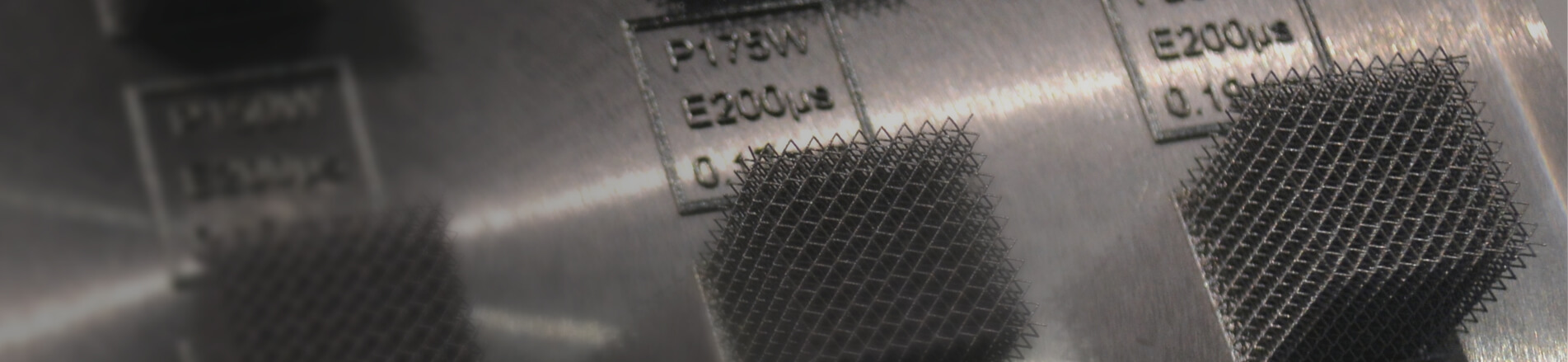
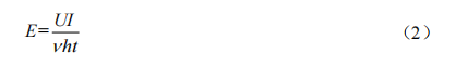
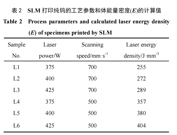
The equipment model used for the SLM forming pure tungsten test is Farsoon271M, the laser wavelength of the equipment is 106 μm, and the spot size is 130 μm. The experimental substrate is 316L stainless steel plate, and the substrate is preheated to 100 ℃ before printing. Nitrogen (purity 99.9%) is filled as a protective atmosphere during the printing process. When the ambient oxygen content is lower than 200 μL/L, the laser forming pure tungsten test begins. The main test parameters: scanning spacing and layer thickness are 70 and 30 μm respectively, and the laser power and scanning speed are shown in Table 2. In order to better evaluate the influence of process parameters, the volume energy density E is used as a measure of the amount of energy in the input sample. The value of E is as follows:
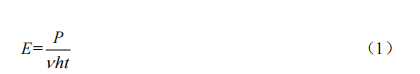
Where P is the laser power, v is the scanning speed, h is the scanning spacing, and t is the thickness of the scanning powder layer.
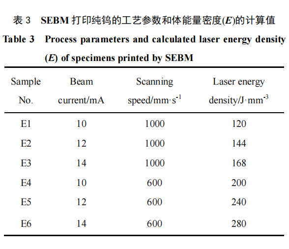
The equipment model for SEBM forming pure tungsten is Sailong S2, the electron beam voltage is constant at 60 kV, and 316L stainless steel plate is used as the substrate. The substrate preheating temperature before printing is 850 ℃. During the printing process, the vacuum is evacuated to 1×10⁻⁴Pa, and then helium (purity 99.9%) is filled to 0.01 Pa. Table 3 shows the specific process parameters and E calculated values of electron beam melting of pure tungsten. The scanning powder layer thickness is 50 μm, the scanning spacing is 100 μm, and the value of the volume energy density E is as follows:
Where, U is the electron beam voltage, I is the electron beam current, v is the scanning speed, h is the scanning spacing, and t is the powder layer thickness.
The density of the printed sample is measured by the Archimedean drainage method, and the density of the pure tungsten sample is calculated. After mechanical grinding and polishing, the samples were corroded with a corrosive solution (10 mL hydrogen peroxide, 10 mL ammonia and 80 mL distilled water) for 90 s, and finally the corroded samples were subjected to microstructural analysis. In this study, an optical microscope (MeF3A) and a scanning electron microscope (JSM-6360LV) were used to observe the surface morphology and microstructure of pure tungsten samples. Electron backscatter diffraction (EBSD) technology was used to analyze the grain size and orientation, and the equipment was a double-beam microscopy system of model Helios Nanolab G3 UC. An X-ray diffractometer (Brucker D8 Discover 2500) was used to perform phase analysis of pure tungsten samples. The microhardness of the sample was measured using a Vickers hardness tester (Buehler 5104, USA), with a load of 200 g and a duration of 10 s.
2 Results and discussion
2.1 Pure tungsten block and macroscopic surface morphology
Figure 2 shows the pure tungsten block formed by SLM and SEBM technology in this study. From the external surface, the overall formability of pure tungsten is good, and there are no obvious defects such as holes and cracks on the surface of the sample.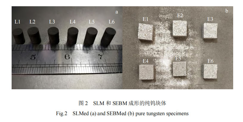
Figure 3 shows the macroscopic surface morphology of the positive surface (perpendicular to the construction direction) of the pure tungsten SLM formed sample under different laser process parameters. It can be seen that with the increase of energy density, the number of surface cracks of the printed sample increases and the pore defects decrease. The cracks are mainly manifested as transverse cracks and longitudinal cracks in the 90° direction, among which the transverse cracks are the junctions of the printed tracks. Additively manufactured pure tungsten materials often have a serious tendency to thermal cracks. On the one hand, it is due to the high ductile-brittle transition temperature of tungsten and its brittle characteristics at room temperature; on the other hand, it is due to the rapid cooling rate and the huge temperature gradient caused during the SLM process. During the laser printing process, there is a large temperature difference between layers, and the cooling rate is fast, resulting in large thermal residual stress. When the residual stress of brittle materials approaches or even exceeds the yield strength of the material itself, it will promote the initiation and expansion of cracks [14,15]. The experimental results show that the temperature gradient in the printed sample can be reduced by optimizing the process parameters and increasing the substrate preheating temperature, thereby reducing the thermal residual stress [16]. Generally, with the increase of laser energy density, the molten pool temperature increases, the temperature gradient and thermal residual stress increase, and the tendency to crack increases.
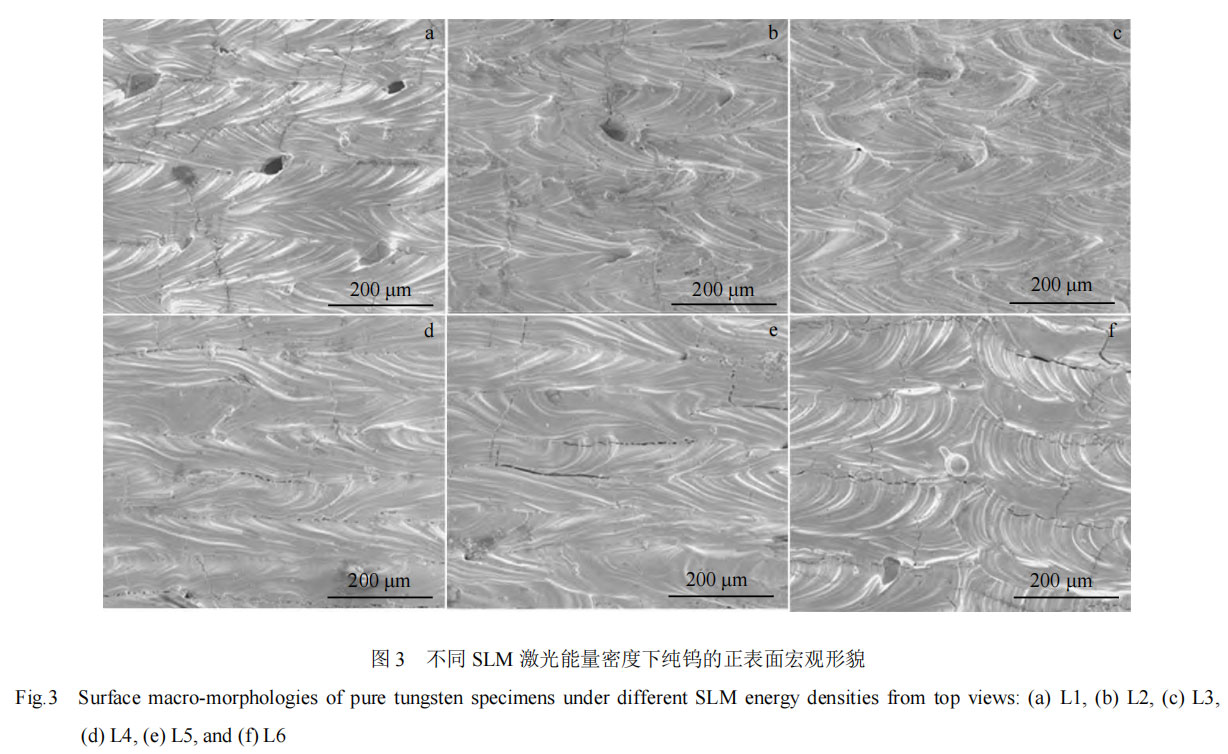
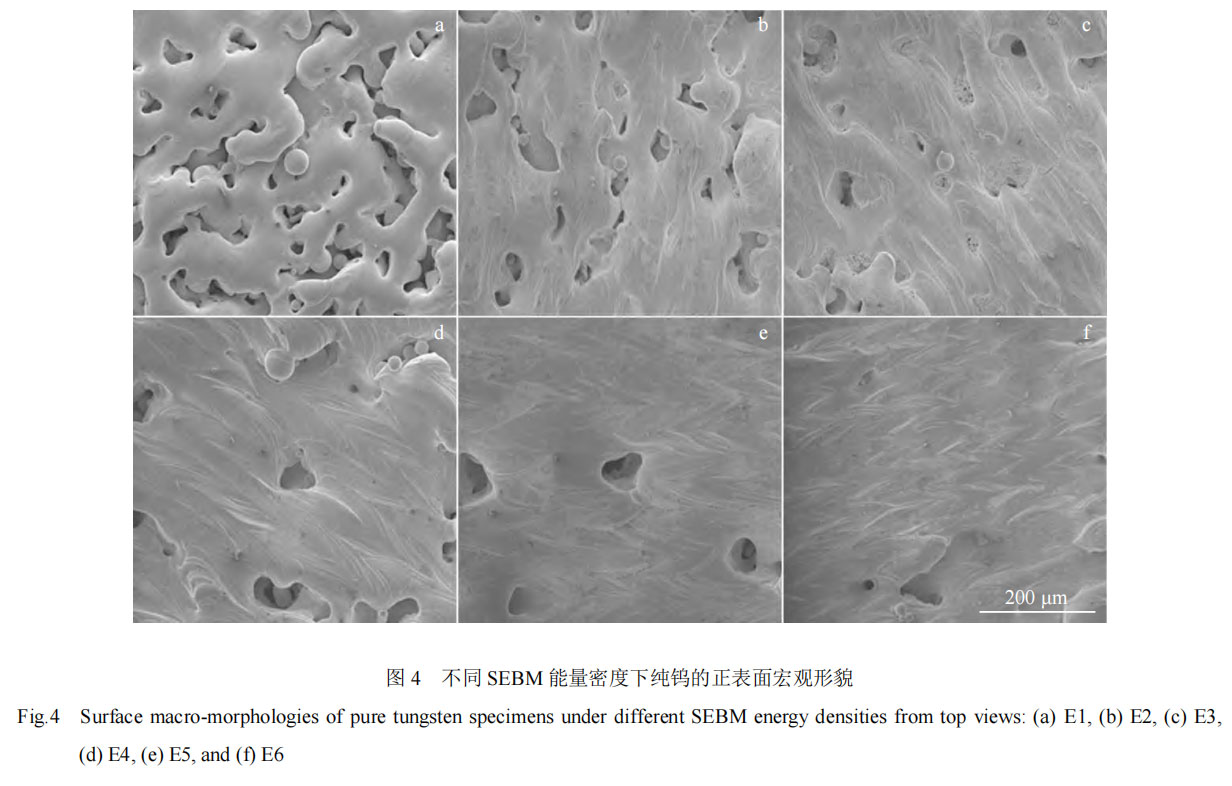
Figure 4 shows the surface macroscopic morphology of SEBM formed samples at different energy densities. With the increase of energy density, the surface of the printed sample changes from a rough surface with a large number of voids, continuous strips or unmelted powder particles (Figure 4a) to a relatively flat and smooth surface (Figure 4d). It can also be seen from Figure 4f that when the energy density reaches 280 J/mm3, the unfused defects are reduced, the spheroidization phenomenon is weakened or even almost absent, and the surface of the formed sample shows a continuous scanning track and uniform structure, indicating that the process parameter control has a great influence on the surface of the pure tungsten formed sample. Appropriately increasing the energy density will be beneficial to the SEBM forming of pure tungsten. The SEBM printing process is a process in which the diffusion and solidification of the powder melt compete with each other. The diffusion of the molten metal is affected by its surface tension and dynamic viscosity. The tungsten metal melt has a higher surface tension and viscosity, resulting in poor wettability and a slower diffusion rate [17,18]. The molten tungsten droplets wet the solid surface at a low speed driven by capillary force, and the large temperature gradient drives it to solidify rapidly. Therefore, the droplets solidify before they are completely diffused and maintain a spherical morphology, rather than forming a flat layer after diffusion. When the energy input to the sample increases, the molten pool temperature increases, the dynamic viscosity of the solution decreases, and the solidification time is longer, so that the droplets can be well diffused, the spreading effect is better, and a smooth and flat surface is formed.
In summary, compared with SLM forming, pure tungsten samples formed by SEBM have higher surface quality and fewer crack defects. During the additive manufacturing process, the cooling rate inside the sample is fast and the temperature gradient is high, which will cause large residual stress, resulting in the generation of cracks inside the sample. The electron beam printing process can better reduce the tendency of thermal cracks [13]. On the one hand, from the printing method, when SEBM prints a layer and spreads the powder, the electron beam will preheat the spread powder and reheat the solidified layer; on the other hand, the high vacuum degree of the molding chamber can allow a very high substrate preheating temperature. During the printing process, the substrate temperature is maintained at about 850 ℃, which can effectively reduce residual stress and reduce the generation of cracks.
2.2 Density and mechanical properties
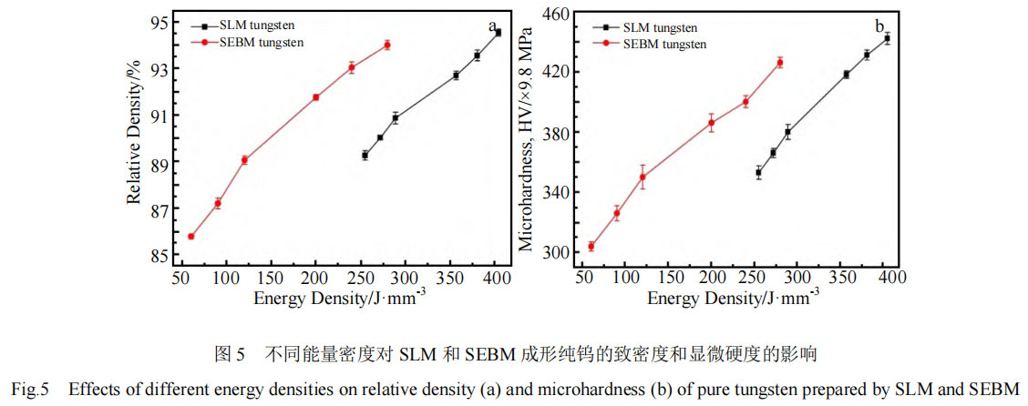
Figure 5 shows the changes in density and microhardness of pure tungsten formed by SLM and SEBM with energy density. Analysis shows that the density and hardness of pure tungsten printed by SLM and SEBM are proportional to the energy density of the input sample. Pure tungsten printed by SEBM can achieve higher density at lower energy density. When the electron beam energy density is 280 J/mm3, the prepared pure tungsten sample reaches a density of 94.3%. When the laser energy is 404.76 J/mm3, the density of the sample is 94.75%. The density largely reflects the number of defects such as pores inside the sample. The formation of pores is because the protective gas in the molding chamber enters the molten pool during the laser melting process and does not have time to overflow, so it remains in the sample to form closed pores. Generally, higher energy density input increases the solidification time of the solution, causing bubbles to escape from the molten pool before solidification. Insufficient laser energy results in limited time for bubbles to escape from the molten pool before solidification, and a reduction in laser energy input will lead to a lack of fusion of the melt, resulting in unfused defects [19]. When SLM is used to prepare pure tungsten samples, although high energy will lead to an increase in macroscopic cracks on the positive surface (Figure 3), there may be fewer microscopic defects such as closed pores inside the sample, so the overall density is higher and the hardness (HV) is also higher, reaching 4174.8 MPa. The SEBM printed pure tungsten sample with fewer pores and defects has a maximum hardness of 4370.8 MPa.
2.3 Microstructure and XRD phase analysis
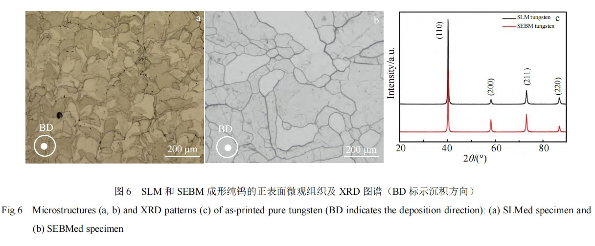
Figure 6 shows the microstructure and XRD spectrum of the positive surface of the pure tungsten samples formed by SLM and SEBM. Similar to Figure 3, it can be seen from the SLM printed pure tungsten structure in Figure 6a that the crack is located at the overlap of the melt channel and the melt channel, which is microscopically manifested as the grain boundary position. In the process of coordinated deformation, the grain boundary is more likely to become a crack source due to its weak ability to resist plastic deformation. Compared with SLM, the pure tungsten grains prepared by SEBM are larger (Figure 6b). This is because the substrate temperature is kept high during printing, the cooling rate is slow, and the energy and time provided for grain growth are more sufficient. At this time, the thermal stress accumulation inside the SEBM printed sample is also small, and the tendency to crack is smaller. As shown in Figure 6c, the physical phases in the SLM and SEBM printed samples are pure tungsten, and there is no tungsten oxide peak.
2.4 EBSD data analysis and crack formation mechanism
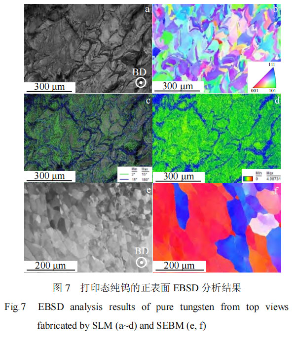
The grain morphology and crack formation mechanism of the SLM and SEM printed pure tungsten samples were further analyzed and studied by characterization using the EBSD technology of the scanning electron microscope. As shown in Figure 7, Figure 7a~Figure 7d are the EBSD analysis results of the SLM printed samples. It can be seen from the scanning microstructure photo in Figure 7a and the inverse pole figure imaging in Figure 7b that the cracks inside the sample are composed of long straight cracks overlapped by the molten pool and cracks extending along the grain boundaries. From the grain boundary orientation morphology in Figure 7c, it can be seen that the grain boundary position where the crack occurs is the large-angle grain boundary (>15°, blue area), while there is almost no crack in the small-angle grain boundary (<15°, green area). It can be calculated that the small-angle grain boundary accounts for 81.8% of the total grain boundary, the large-angle grain boundary accounts for 18.2%, and the average grain size is 56 μm. Figure 7d is the average orientation difference morphology. The blue area represents the position with a small orientation difference, which indicates that there are microcracks at this position, while the green position has a large average orientation difference, which is a stress concentration area. At the same time, the strength is higher in the area near the crack, which indicates that the stress near the crack is large, resulting in cracks.
Figures 7e and 7f are the EBSD results of SEBM printed pure tungsten, respectively. Calculation shows that the average grain size of the SEBM pure tungsten sample is 175.3 μm, the small-angle grain boundary accounts for 98.7%, and the large-angle grain boundary accounts for 1.3%. Compared with SLM, the grains of pure tungsten prepared by SEBM are coarser overall, and the proportion of small-angle grain boundaries is higher. Small-angle grain boundaries can effectively hinder the further propagation of cracks, while the stress near large-angle grain boundaries is relatively high, which is easy to become the source of cracks, thereby causing intergranular cracks.
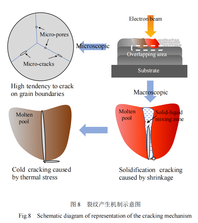
Combining the above results and the reports of existing researchers [14,15], the schematic diagram of the crack formation mechanism shown in Figure 8 is constructed to explain the location and mechanism of crack initiation inside pure tungsten samples prepared by additive manufacturing. Macroscopically speaking, cracks in pure tungsten samples mostly initiate in the overlap area. The forming of block specimens requires overlap of channels or layers, and the impact of overlap is that the molten pool has two directions of heat dissipation trends: one is longitudinal heat dissipation through the substrate; the other is lateral heat dissipation through the adjacent solidified deposition layer, resulting in a lateral temperature gradient. At this time, the cracks are formed during the solidification shrinkage process and are generated in the solid-liquid mixing zone at the final stage of solidification. At this time, there are solidification shrinkage pores near the solid phase zone in the mixing zone. The pores are very likely to produce local stress concentration, thus more likely to promote the formation of cracks [20].
The internal temperature of the sample decreases, and pure tungsten is brittle at low temperatures (200-400 °C). The thermal stress generated during solidification will also cause low-temperature cracking. From a microscopic perspective, cracks have the characteristics of extending along the grain boundaries. This is because the grain boundary speed filled by the liquid phase cannot keep up with the solidification speed or the crack formation speed. As the solidification proceeds, the liquid film of the residual liquid phase is torn under the action of thermal stress, thus forming cracks.
3 Conclusion
1) The density and hardness of pure tungsten formed by SLM and SEBM are positively proportional to the energy density of the input sample. The density of pure tungsten formed by SLM reaches up to 94.3%, and the hardness (HV) reaches 4174.8 MPa. The density of pure tungsten formed by SEBM reaches up to 94.75%, and the hardness (HV) reaches 4370.8 MPa.
2) Compared with SLM, pure tungsten formed by SEBM has fewer microcracks.
The internal cracks of SLM samples mostly exist in the overlap area. The cracks generated during the preparation of SLM and SEBM are characterized by distribution along the grain boundaries.
3) From the perspective of the crack generation mechanism, cracks mostly initiate at high-angle grain boundaries. Compared with SLM, the high-angle grain boundaries of SEBM printed samples account for a smaller proportion and the number of low-angle grain boundaries is larger, so the tendency to form cracks is smaller. During the SEBM forming process, the matrix is always kept at 850 ℃, so the grains are easy to grow, the temperature gradient is also small, the thermal stress is smaller, and it is not easy to crack.
Paper citation information
Volume 51, No. 9 September 2022
RARE METAL MATERIALS AND ENGINEERING
Vol.51, No.9
September 2022
Stardust Technology not only supplies high-purity rare refractory metal spherical powders, including spherical tungsten powder, molybdenum powder, niobium powder, tantalum powder, vanadium powder, rhenium powder, etc. The powder has stable quality, uniform particle size and excellent fluidity! We also provide integrated solutions for metal 3D printing rapid prototyping, from design modeling to finished product delivery, one-stop service! Whether it is aerospace, electronic information, or medical equipment, we can accurately meet your various high-end manufacturing needs!
Contact Vicky for more details! +86-13318326185


Signup our newsletter to get update information, promotion and insight.


 IPv6 network supported